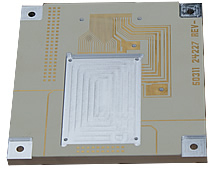
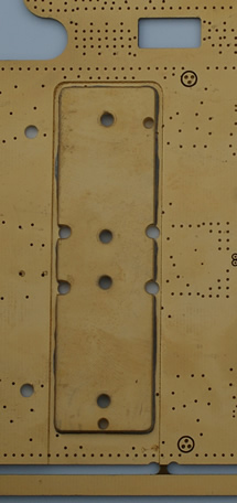
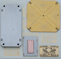
Delta Circuits provides a complete one-source solution to your manufacturing requirements through our comprehensive... changing demands of the electronic industries latest technologies.
RF (Radio Frequency Boards)

- Top to Bottom Alignment .0005" Same Layers
- Etching ±.0005" (1/2 Oz. Copper)
- .001" Spacing
- Measuring Capability for Coupling, Filters, Impendance, Differential Pair measurements in house
Power Amplifier Boards

- Mix Dielectric Multilayer
- Highly Thermally Conductive Materials
- Cavity under Power transistor launch area for RF Ground and edge plating
- Selective Plating
- Selective Edge Plating
Conductive Thermal or Electrical Adhesive

- 2-5 mil Thickness Conductive adhesive
- Selectively Applied Adhesive
- Pre cut or Pre Forms
- Post and Pre fab after attachment
- Vertical Machining Center Capability
- DC Resistance measurement Capability
Sweat Soldering

- Temperature range from 165 deg C- 290 deg C Solder.
- Selectively Specified area to be attached.
- Complex Board connection with metal carrier.
- Metal Coins at power transistor area.
- Metal back board attached to base plate.
High Count Layers Ceramic filled Multilayer Boards (Certified MIL-PRF-55110,Type 3)

- 36 Layers Ceramic filled multilayer
- Homogeneous Prepreg
- Precise Layer to Layer Registration
- X-ray measurement Capability for layer movement and layer to layer registration.
Fusion Bonding

- 24 Layers Teflon Fusion Bonding Capability (24" X 24")
- Same Dielectric Constant and Material Properties since fusing the same material as core.
- Good Control with material movement in X,Y & Z directions.
FEP Bonding

- Pure FEP Bonding , Very low loss .0002
- Excellent at high frequency
High Power RF Component Boards

- Up to 0.500" thick multilayer boards
- Cavity to middle layer for RF Connection
- Hole Castellation
- Selective Edge plating for RF Grounding
Printed Antenna on Multilayer Boards

- ±.0005" Line Width Tolerances.
- ± .0005" Spacing Tolerances
- Cavity mount for Circulators.
- Single Side 36" X 100" largest Size board
Back Plane

- Double and Multilayer largest board size 30" X 52"
- Back Plane Layers up to 48
- Largest board size 30" X 52"
- Aspect Ratio of 18:1
Microvia

- Smallest Platted vias 1.9 mil (Laser or Mechanical drilling)
- Via Filled with Non Conductive and Conductive Epoxy
- Vial Plate and Shut.
- Via in Pad with Caps
- 18:1 Aspect Ratio Panel to Drill(Pulse Plating Rectifier)
Blind /Buried Vias

- Blind, Buried vias and Blind/Buried Vias
- Sequential Lamination
- Depth Control drilling/Laser depth control 1:1 Ratio
- Mix Dielectric: Combination of Teflon, Getek, Rogers Duroid 4350, Nelco 400, NL 2000, FR 406 & 408 & many more
- Selective to pocket depth in layers for immediate RF ground for power transistor or metal slugs.
BGA

- 20 mil ball grid array
- 100% electrical testing with Flying Probe or Electrical Fixture.
- With Via in Pad
- With micro vias.
Surface Finisher

- Electroless Nickel and Immersion Gold
- Immersion Tin
- HASL,OSP,Virgin Tin,Bare Copper
- Wire Bondable Gold
Rigid /Flex

- Flex
- Flex Multilayer
- Rigid/Flex
Thin Laminates
- 0.002"- .005"
- Critical Geometry
Single Side Antenna Boards
- up to 96" long board
MEDICAL

AEROSPACE

COMPUTING


